980 nm High Power FP Laser Diode Epi-Wafer
- Product Item : HYRD-W002
- Category: Wafers
- Thickness control: <5%
- Thickness uniformity: <3%
- PL wavelength uniformity: <3 nm
- Doping control: <30%
980 nm High Power FP Laser Diode Epi-Wafer
PRODUCT DESCRIPTION
The 980 nm Fabry-Perot (FP) laser diode (LD) epi-wafer, designed especially for the high-power characteristics, is grown by metal-organic chemical vapor deposition (MOCVD), with strained InGaAs quantum well as the active layer.
EPITAXY STRUCTURE
p+-GaAs Contact
p-AlGaAs Cladding
Waveguide
Active layer
Waveguide
n-AlGaAs Cladding
n-GaAs Buffer
n-GaAs Substrate
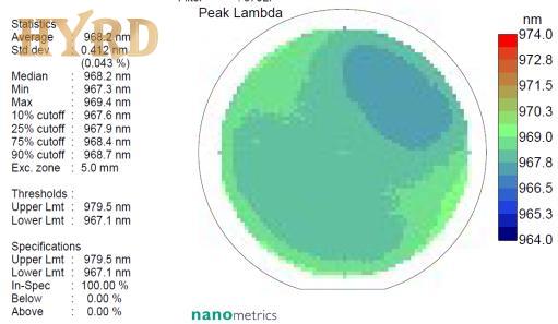
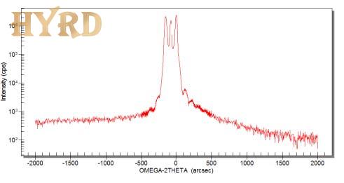
WAFER CHARACTERIZATION
PRODUCT DESCRIPTION
The 980 nm Fabry-Perot (FP) laser diode (LD) epi-wafer, designed especially for the high-power characteristics, is grown by metal-organic chemical vapor deposition (MOCVD), with strained InGaAs quantum well as the active layer.
EPITAXY STRUCTURE
p+-GaAs Contact
p-AlGaAs Cladding
Waveguide
Active layer
Waveguide
n-AlGaAs Cladding
n-GaAs Buffer
n-GaAs Substrate
WAFER CHARACTERIZATION
|
Photoluminescence (PL) of 3-inch epi-wafer |
X-ray diffraction (XRD) of 3-inch epi-wafer |
TYPICAL EPITAXY PARAMETERS
Parameters
Values
Thickness control
<±5%
Thickness uniformity
<±3%
PL wavelength uniformity
<±3 nm
Doping control
<±30%
Mole Fraction (x) Tolerance
<±2%
TYPICAL DEVICE PERFORMANCE
Parameters
Typical Values
Threshold current@25℃
65mA
Wavelength
980 nm
Slope efficiency
0.55 W/A
Ridge waveguide
30 μm x 1000 μm,
as cleaved facet @ RT
KEY FEATURES
* MOCVD Epitaxy.
* 2/3/4/6 Inch.
* Excellent Beam Quality.
* High Power & Efficiency.
* High Uniformity & Reliability.
APPLICATIONS
* Materials Processing.
* Laser Pumps.
* Medical / Aesthetics
Our company can provide compound semiconductor optoelectronic epitaxial wafers, mainly based on advanced semiconductor technology to prepare optoelectronic epitaxial wafers with different structures and functions using indium phosphide (InP) and gallium arsenide (GaAs) as substrates, widely used in fields such as communication and medical aesthetics.
RELATED PRODUCTS: