1310 nm 2.5G FP Laser Diode Epi-Wafer
- Product Item : HYRD-W004
- Category: Wafers
- Threshold current@25℃:<10mA
- Wavelength: 1310 nm
- Slope efficiency: 0.25 W/A per facet
- Characteristic temperature: >85 K
1310 nm 2.5G FP Laser Diode Epi-Wafer
PRODUCT DESCRIPTION
The 1310 nm Fabry-Perot (FP) laser diode (LD) epi-wafer, designed especially for the high-speed fiber-optic communications, is grown by metal-organic chemical vapor deposition (MOCVD), with strained InAlGaAs or InGaAsP multiple quantum wells (MQWs) as the active layer.
EPITAXY STRUCTURE
p+-InGaAs Contact
p-InP Cladding
Waveguide
MQWs
Waveguide
n-InP Cladding
n-InP Buffer
n-InP Substrate
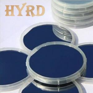
WAFER CHARACTERIZATION
Photoluminescence (PL) of 2-inch epi-wafer
X-ray diffraction (XRD) of 2-inch epi-wafer


TYPICAL EPITAXY PARAMETERS
Parameters
Typical Values
Thickness control
<±5%
Thickness uniformity
<±3%
PL wavelength uniformity
<±5 nm for 2-inch Epi-wafer
Doping control
<±30%
p-InP carrier concentration
1E17 cm-3 ~ 2E18 cm-3
n-InP carrier concentration
1E16 cm-3 ~ 5E18 cm-3
p-InGaAs carrier concentration
1E19 cm-3 ~ 2E19 cm-3
TYPICAL DEVICE PERFORMANCE
Parameters
Typical Values
Threshold current@25℃
<10mA
Wavelength
1310 nm
Slope efficiency
0.25 W/A per facet
Characteristic temperature
>85 K
Serial resistance
<10 Ω
Operating temperature
-20℃ ~ +85℃
Ridge waveguide
2 μm x 250 μm, as cleaved
KEY FEATURES
⚫ MOCVD Epitaxy.
⚫ 2/3/4 Inch.
⚫ 2.5G High-Speed.
⚫ High Uniformity & Reliability.
APPLICATIONS
⚫ Telecommunications
Our company can provide compound semiconductor optoelectronic epitaxial wafers, mainly based on advanced semiconductor technology to prepare optoelectronic epitaxial wafers with different structures and functions using indium phosphide (InP) and gallium arsenide (GaAs) as substrates, widely used in fields such as communication and medical aesthetics.