850 nm Vcsel Laser Diode EPI-Wafer
- Product Item : HYRD-W003
- Category: Wafers
- SB center: <±10 nm
- Thickness uniformity: <±2.5%
- PL wavelength uniformity: <±1.5 nm
- Mole Fraction (x) Tolerance : <±2%
850 nm Vcsel Laser Diode EPI-Wafer
PRODUCT DESCRIPTION
The 850 nm vertical-cavity surface-emitting laser (VCSEL) epi-wafer, designed especially for the telecommunication/gesture recognition/3D imaging applications, is grown by metal-organic chemical vapor deposition (MOCVD), with GaAs/AlGaAs multiple quantum wells (MQWs) as the active layer.
EPITAXY STRUCTURE
p+-GaAs
P-AlGaAs
P-DBR
Al0.98GaAs
MQWs
AlGaAs
n-DBR
n-GaAs buffer layer
n-GaAs substrate
WAFER CHARACTERIZATION
PRODUCT DESCRIPTION
The 850 nm vertical-cavity surface-emitting laser (VCSEL) epi-wafer, designed especially for the telecommunication/gesture recognition/3D imaging applications, is grown by metal-organic chemical vapor deposition (MOCVD), with GaAs/AlGaAs multiple quantum wells (MQWs) as the active layer.
EPITAXY STRUCTURE
p+-GaAs
P-AlGaAs
P-DBR
Al0.98GaAs
MQWs
AlGaAs
n-DBR
n-GaAs buffer layer
n-GaAs substrate
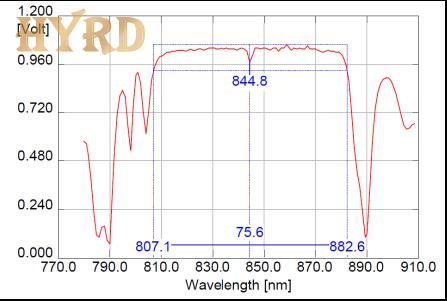
WAFER CHARACTERIZATION
|
Reflectivity spectrum of 4-inch epi-wafer |
Concentration depth profile of 4-inch epi-wafer |

TYPICAL EPITAXY PARAMETERS
Parameters
Typical Values
SB center
<±10 nm
Thickness uniformity
<±2.5%
PL wavelength uniformity
<±1.5 nm
Doping control
<±30%
Mole Fraction (x) Tolerance
<±2%
TYPICAL DEVICE PERFORMANCE
Parameters
Typical Values
Threshold current@25℃
< 2 mA (15μm aperture)
Wavelength
845-855 nm
Slope efficiency
> 0.5 W/A
Operating temperature
0℃ ~ 80℃
KEY FEATURES
⚫ MOCVD Epitaxy.
⚫ 2/3/4 Inch.
⚫ 2.5G High-Speed.
⚫ High Uniformity & Reliability.
APPLICATIONS
⚫ Telecommunications
Our company can provide compound semiconductor optoelectronic epitaxial wafers, mainly based on advanced semiconductor technology to prepare optoelectronic epitaxial wafers with different structures and functions using indium phosphide (InP) and gallium arsenide (GaAs) as substrates, widely used in fields such as communication and medical aesthetics.